The ICS525 Programmable Clock Synthesizer
I'm working on a TAPR project called the Clock-Block. It's a simple synthesizer designed for applications like controlling the frequency of a PC's clock for timekeeping purposes. This page has some info about the ICS525 programmable clock synthesizer that is at the heart of the design.
The TAPR Clock-Block Prototype
NOTE: The production board will look a bit different than this. Among other things, the two rows of headers have been replaced by two DIP switches, two mounting holes have been added, dual supply (3.3 or 5 volt) operation is supported, and traces are provided to install an optional divider that allows use in the audio to LF range.
The Heart of the Matter
The ICS525 is a versatile chip that accepts a clock input from 2 to 50MHz and can produce an output frequency from 5 to 250MHz (using the -02 variant).It's designed as a clock for timing, and not as an RF synthesizer.
Set to operate in "lowest jitter" mode with a 10MHz input clock and
programmed for 200MHz output, all non-harmonic spurs are >50dB down. Even
harmonics and subharmonics tend to run between -50 and -60dB.
The ICS525 comes in 2 variants (there are actually more, but they don't
seem to be readily available. The -01 is a lower performance device; the
-02 has a higher operating frequency and less jitter.
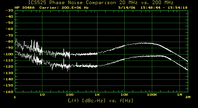
Comparing two output frequencies an order of magnitude apart shows that
the phase noise reduces about 20dB.
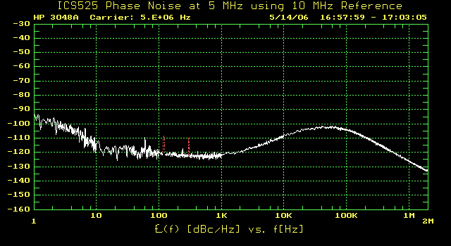
Reducing the output frequency still further shows yet more noise
reduction:
Following is an example of a very different noise signature. In this case,
the divisor ratios were much more complicated than in the other examples,
and in particular the R (reference) divider was set to 25; the other
frequencies did not use the R divider.
Finally, here is a spectrum analyzer screenshot that more vividly depicts
the noise. The red trace is the ICS525 at 250MHz, driven by an HP Z3801A
GPSDO which has pretty good phase noise. The cyan trace is a Marconi
2202A signal generator driven by the same Z3801A. While the 2202A isn't a
lab-grade instrument and has only modest phase noise performance, you can
see that it's dramatically better than the ICS525:
Brooke Clarke's
Battery Top Signal Generator page has some really good information
about programming the ICS525. Brooke believes, and it makes sense to me,
that for lowest jitter you want to use the divisor combination that has
the highest output ("S") divisor; if there's a tie, then pick the lowest
VCO ("V") divisor.
If you want to do it the simple way, there's an
ICS525
calculator at the ICS web site that will show you the divider settings
for a given input and output frequency. Note that it asks you to specify
the permissible frequency error; the chip doesn't have unlimited resolution
and some frequencies cannot be generated precisely.
Also note that the generator won't let you enter input or output values
outside the specified range for the chip; Brooke has shown that you can go
quite a bit outside that range if you're willing to work out the divisor
settings manually.
Below are jumper settings for several frequencies using the ICS525-02 in
the "lowest jitter" configuration from the calculator. (By the way, the
-01 chip has a slightly different divider arrangement; its progamming is
different than the -02. The calculator provides information for both
variants.)
Out Freq S2 S1 S0 R6 R5 R4 R3 R2 R1 R0 V8 V7 V6 V5 V4 V3 V2 V1 V0 14.318182MHz 0 1 0 0 0 0 1 0 0 1 0 0 0 1 1 0 1 1 1 20MHz 0 1 0 0 0 0 0 0 0 0 0 0 0 0 0 1 0 0 0 33.33...MHz 0 0 0 0 0 0 0 0 0 0 0 0 0 0 0 1 1 0 0 50MHz 0 1 0 0 0 0 0 0 0 0 0 0 0 1 0 0 0 0 0 100MHz 0 1 1 0 0 0 0 0 0 0 0 0 0 1 0 0 0 0 0 200MHz 0 0 1 0 0 0 0 0 0 0 0 0 0 1 0 0 0 0 0 250MHz 1 1 0 0 0 0 0 0 0 0 0 0 0 0 1 0 0 0 1
Phase Noise Measurements
The plot below shows noise out to 40MHz; all the other plots go out to
2MHz (due to measurement limitations at lower frequencies).


Progamming
The chip uses three dividers, denominated as S, R, and V. The divisors
are set by parallel pins with internal pull-ups. That means by default
the pins are set to 1; to set a zero, ground the pin. Don't make the
mistake I did and assume in the programming charts below that a 1 means to
install a shorting block!
Input Frequency = 10MHz